Different types of semiconductors
In our previous article, we looked at the characteristics of a semiconductor. We’re now going to move on to looking at different types of semiconductors and how they work.
N-type and P-type semiconductors
The image below shows an n-type conductor:

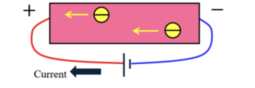
Phosphorus has one more electron than silicon does, so when it replaces some silicon atoms within the crystal, this “extra” electron is free to move when a voltage is applied. The electron, which is negative, is attracted towards the positive terminal, creating a current:
The image below shows a p-type conductor:

Boron has one fewer electron than silicon, so when it replaces some silicon atoms within the crystal, it leaves a space, or vacancy, where there is no electron. This vacancy is called a hole, and it can be classified as a virtual particle.
How does current flow in a p-type semiconductor?
In this conductor, the holes appear to be moving. The neighbouring electron is then pulled towards the hole to fill it. When the electron has moved into the hole, it leaves behind a new hole, as you can see in the image below:

This process is repeated, creating holes in the Boron and Silicon.
As this process is repeated, electrons move towards the positive pole while holes move towards the negative pole. Only the electrons are actually moving, but the holes have positively charged particles:

As a result, both p-type and n-type semiconductors can have current flow, but they aren’t as conductive as metal. What this means, is that we would have no use for semiconductors if the only purpose was current flow or conductivity.
The advantages of a semiconductor include its ability to allow or stop current flow based on certain conditions. In fact, the basic principle behind a semiconductor is in its rectification behaviour using a p-n junction.
Forward Bias
Voltage is applied in the forward direction of the p-n junction:

When the voltage is applied to the p-n junction, the holes and electrons can be moved towards the interface.
When holes and electrons meet at the interface, the electrons jump into holes and both are eliminated. After those electrons are eliminated, more flow into the n-layer, and electrons flow out from the p-layer, creating new holes. This is repeated, enabling the current to continue to flow.
Reverse Bias
Voltage is applied in the reverse direction of the p-n junction:

Here is the region that doesn’t have any holes or electrons, called the depletion layer. Voltage is applied to the p-n junction so that n becomes plus. Since the holes and electrons move away from one another, they don’t meet at the interface, and the current can’t flow.
A region forms close to the interface, called the depletion layer, which doesn’t have any holes or electrons, and this produces voltage-withstanding. This lets us know that there is rectification behaviour in the p-n junction.
Keep an eye out for our next articles, which will give you even more interesting facts on semiconductors and their characteristics.
Interested in our courses?
You can read more about our selection of accredited online electrical and electronic engineering courses here.
Check out individual courses pages below:
Diploma in Electrical and Electronic Engineering
Higher International Certificate in Electrical and Electronic Engineering
Diploma in Electrical Technology
Diploma in Renewable Energy (Electrical)
Higher International Diploma in Electrical and Electronic Engineering
Alternatively, you can view all our online engineering courses here.
Recent Posts
Civil Engineering Courses and Diplomas: Topics, Skills and Career Routes
Civil Engineering Courses and Diplomas: Topics, Skills and Career Routes Introduction Civil engineering is the backbone of modern society. From roads and bridges to skyscrapers and water systems, civil engineers design, build, and maintain the infrastructure that keeps the world running. If you’re considering a civil engineering course or diploma, understanding what it covers is […]
What Is a Diploma in Engineering? Courses, Levels and Career Routes Explained
What Is a Diploma in Engineering? Courses, Levels and Career Routes Explained Introduction Engineering shapes the world around us, from the buildings we live in to the technology we use every day. But for many aspiring engineers, the biggest question is not whether to pursue engineering, but how to start. Traditional university degrees are not […]
Engineering Courses: How to Choose the Right Route for Your Career
Engineering Courses: How to Choose the Right Route for Your Career Introduction Choosing an engineering course can feel like standing at the beginning of several different roads, each leading towards a different kind of future. One route may lead into mechanical systems and manufacturing. Another may lead towards aircraft, infrastructure, electronics, computing, renewable energy or […]