The operation of metal oxide semiconductors
In our previous article, we discussed how semiconductors operate. We’re now going to get a bit more specific and look in detail at metal oxide semiconductors.
Junction Field-effect Transistors (JFET)
We first need to understand Junction Field-effect Transistors before focusing on a metal oxide semiconductor.
A transistor is a linear semiconductor device that controls current with the application of a lower-power electrical signal. Transistors can be grouped into two major groups: bipolar and field-effect.
All field-effect transistors are unipolar devices and the main current through them is either electrons through an N-type semiconductor or holes through a P-type semiconductor. This becomes more evident when a physical diagram of the device is seen. The diagram below shows the n-channel JFET:
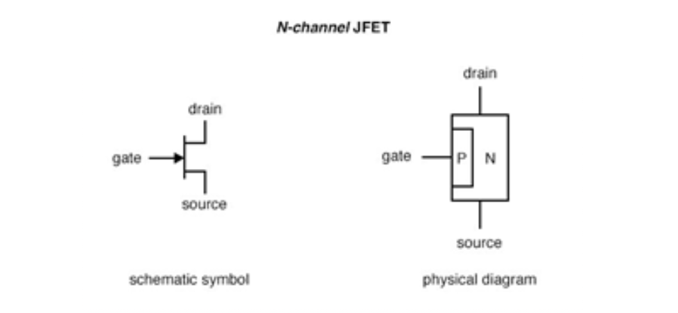
In a JFET, the controlled current passes from source to drain, or from drain to source. The controlling voltage is applied between the gate and source. The current doesn’t have to cross through a PN junction on its way between source and drain: the path, known as a channel, is an uninterrupted block of semiconductor material.
The diagram below shows the p-channel JFET:
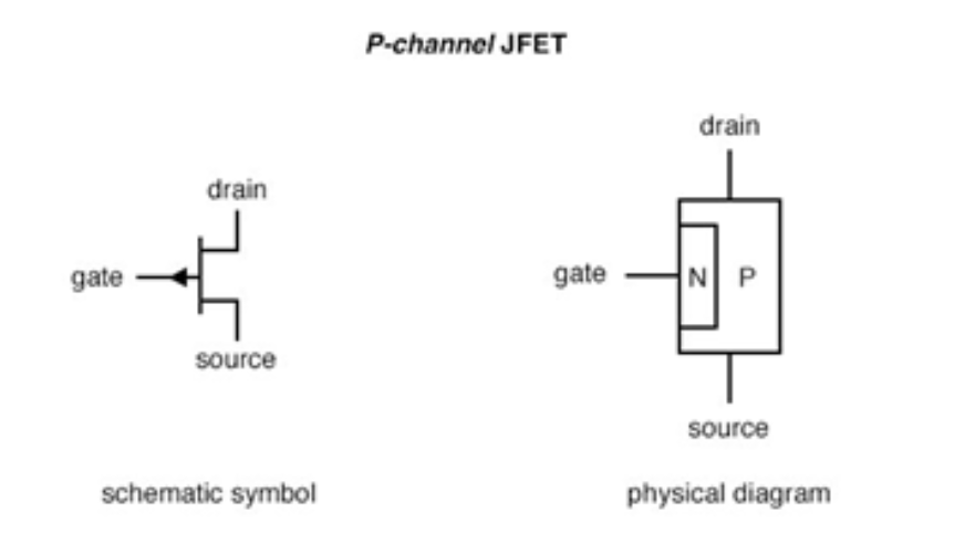
Normally, n-channel JFETs are more commonly used than the p-channel JFETs.
Operational characteristics
The main difference between n-channel and p-channel JFETs is biasing of the PN junction formed between the gate material and the channel. With no voltage applied, the channel is a wide-open path for current to flow.
However, if a voltage is applied between gate and source of such polarity that it reverse-biases the PN junction, the flow between source and drain connections becomes limited or regulated.
Maximum gate-source voltage “pinches off” all current through source and drain, thus forcing the JFET into cut-off mode.
This behaviour is due to the depletion region of the PN junction expanding under the influence of a reverse-bias voltage, eventually occupying the entire width of the channel if the voltage is great enough.
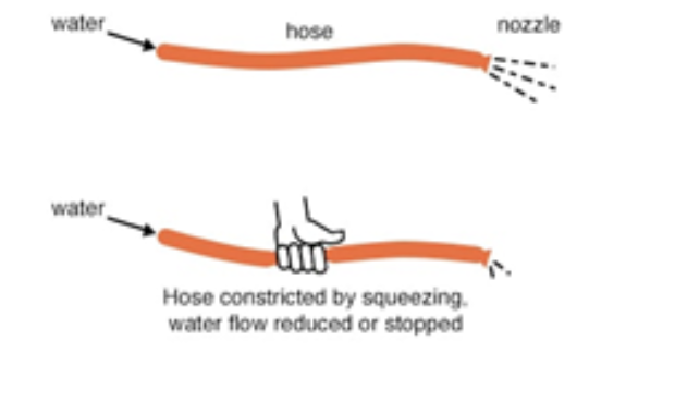
Another way to think about it is by picturing reducing the flow of a liquid through a flexible hose by squeezing it: with enough force, the hose will be constricted enough to completely block the flow.
Metal Oxide semiconductor field effect transistor (MOSFET)
The most common type of Insulated Gate Field Effect Transistor (IGFET) is the metal oxide semiconductor field transistor (MOSFET).
The MOSFET or IGFET is a voltage-controlled field effect transistor that differs from a JFEET. The MOSFET has a metal oxide gate electrode which is electrically insulated from the main semiconductor n-channel or p-channel by a very thin layer of insulating material, usually glass.
This ultra-thin insulated metal gate electrode can be thought of as one plate of a capacitor. The isolation of the controlling Gate makes the input resistance of the MOSFET extremely high (MΩ) region thereby making it almost infinite.
As the Gate terminal is electrically isolated from the main current carrying channel between the drain and source, no current flows into the gate, and just like the JFET, the MOSFET also acts like a voltage-controlled resistor where the current flowing through the main channel between the Drain and Source is proportional to the input voltage.
Both the JFET and the MOSFETs are susceptible to large amounts of static charge, so easily damaged.
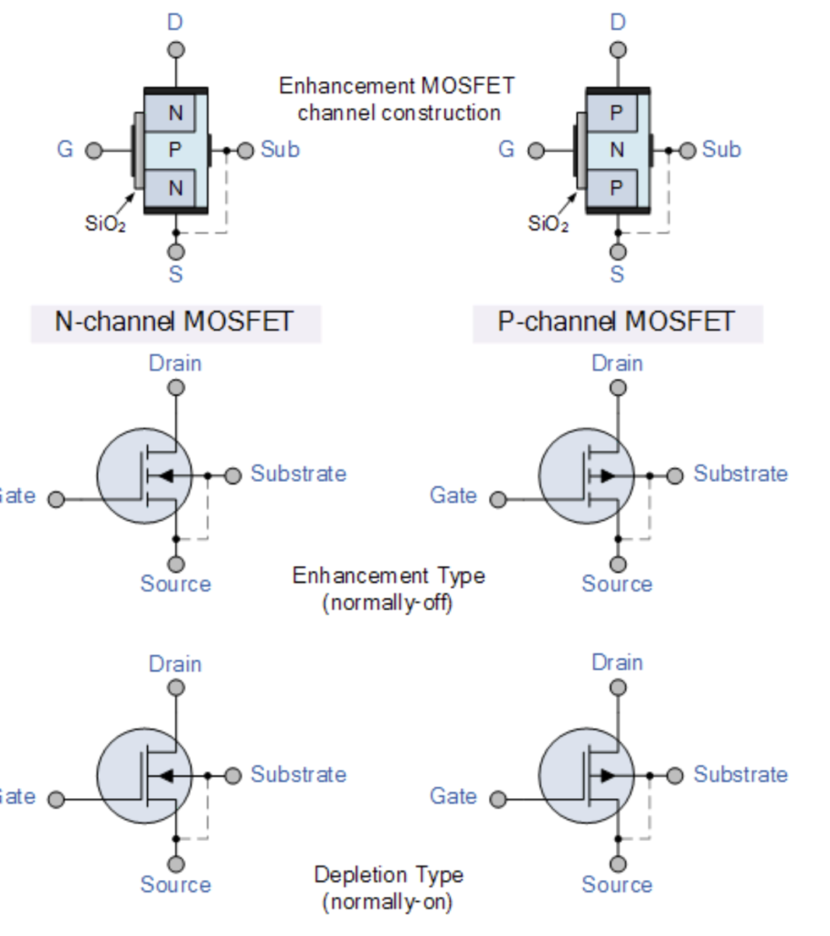
MOSFETs are three terminal devices with a Gate, Drain and Source and both P-channel (PMOS) and N-channel (NMOS) MOSFETs are available. The main difference this time is that MOSFETs are available in two basic forms:
- Depletion Type – the transistor requires the Gate-Source voltage, (VGS) to switch the device “OFF”. The depletion mode MOSFET is equivalent to a “Normally Closed” switch.
- Enhancement Type – the transistor requires a Gate-Source voltage, (VGS) to switch the device “ON”. The enhancement mode MOSFET is equivalent to a “Normally Open” switch.
The image below shows the symbols and construction for both configurations of MOSFETs:
Basic MOSFET Structure
Both the Depletion and Enhancement type MOSFETs use an electric field produced by a gate voltage to alter the flow of charge carriers, electrons for n-channel or holes for P-channel, through the semiconductive drain-source channel. The image below shows this:
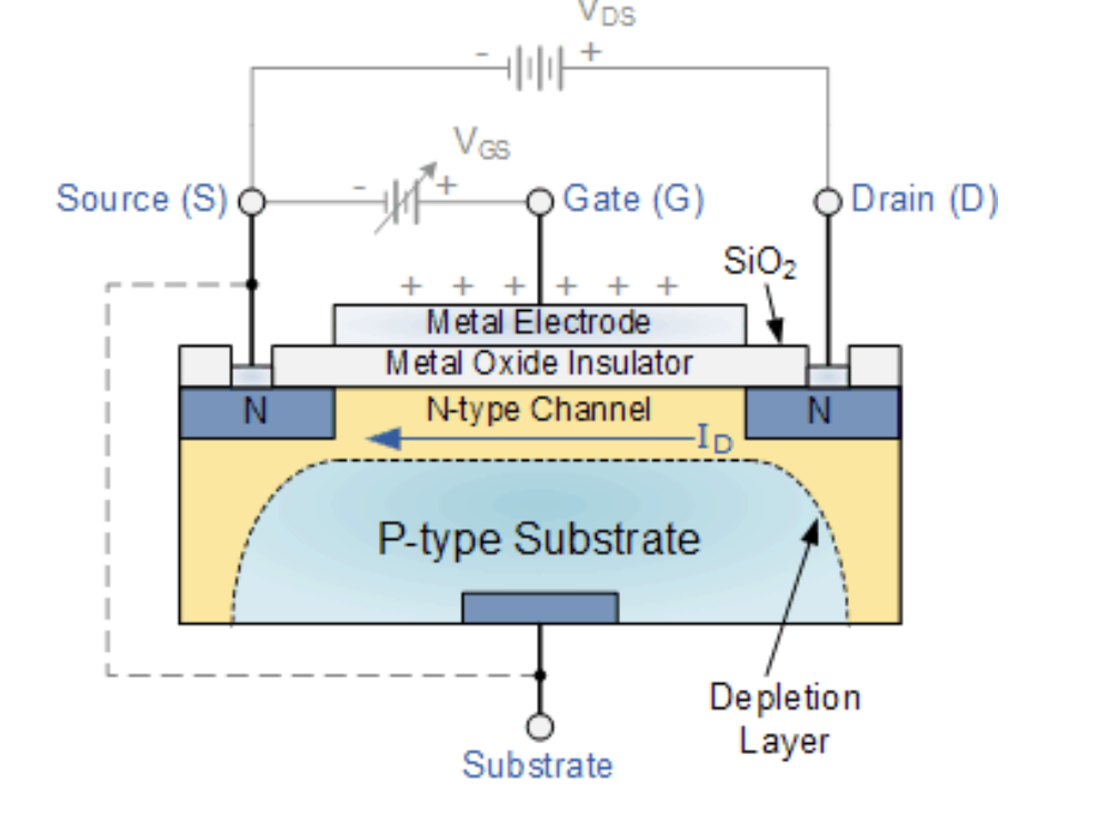
The gate electrode is placed on top of a very thin insulating layer and there are a pair of small n-type regions just under the drain and source electrodes.
With an insulated gate MOSFET device no such limitations apply so it is possible to bias the gate of a MOSFET in either polarity, positive (+ve) or negative (-ve).
This makes the MOSFET device especially valuable as electronic switches or to make logic gates because with no bias they are normally non-conducting and this high gate input resistance means that very little or no control current is needed as MOSFETs are voltage controlled devices.
Both the p-channel and the n-channel MOSFETs are available in two basic forms, the Enhancement type and the Depletion type.
Keep an eye out for our next article looking at another type of semiconductor
Interested in our courses?
You can read more about our selection of accredited online electrical and electronic engineering courses here.
Check out individual courses pages below:
Diploma in Electrical and Electronic Engineering
Higher International Certificate in Electrical and Electronic Engineering
Diploma in Electrical Technology
Diploma in Renewable Energy (Electrical)
Higher International Diploma in Electrical and Electronic Engineering
Alternatively, you can view all our online engineering courses here.
Recent Posts
Civil Engineering Courses and Diplomas: Topics, Skills and Career Routes
Civil Engineering Courses and Diplomas: Topics, Skills and Career Routes Introduction Civil engineering is the backbone of modern society. From roads and bridges to skyscrapers and water systems, civil engineers design, build, and maintain the infrastructure that keeps the world running. If you’re considering a civil engineering course or diploma, understanding what it covers is […]
What Is a Diploma in Engineering? Courses, Levels and Career Routes Explained
What Is a Diploma in Engineering? Courses, Levels and Career Routes Explained Introduction Engineering shapes the world around us, from the buildings we live in to the technology we use every day. But for many aspiring engineers, the biggest question is not whether to pursue engineering, but how to start. Traditional university degrees are not […]
Engineering Courses: How to Choose the Right Route for Your Career
Engineering Courses: How to Choose the Right Route for Your Career Introduction Choosing an engineering course can feel like standing at the beginning of several different roads, each leading towards a different kind of future. One route may lead into mechanical systems and manufacturing. Another may lead towards aircraft, infrastructure, electronics, computing, renewable energy or […]