The structure and mechanism of a Bipolar transistor
In our previous article, we discussed the operation of metal oxide transistors, and now we’re going to have a look at bipolar transistors. We’ll look at their mechanism and how they work.
What is a bipolar transistor?
A bipolar junction transistor is a semiconductor device which can be used for switching or amplification.
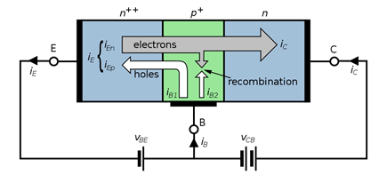
Signal diodes are made up from two pieces of semiconductor material, to form a simple p-n junction. If we join together two signal diodes back-to-back, this will give us two pn-junctions, connected together in series, which share a common Positive (P) or Negative (N) terminal.
The fusion of these two diodes produces a three-layer, two junction, three terminal device, which forms the basis of a Bipolar Junction Transistor (BJT):
Transistors are three terminal active devices made from different semiconductor materials that act as either an insulator or a conductor by the application of a small signal voltage.
The transistor’s ability to change between these two states allows it to have two functions: “switching” (digital electronics) or “amplification” (analogue electronics).
Bipolar transistors have the ability to operate within three different regions:
- Active Region: the transistor operates as an amplifier and Ic = β*Ib
- Saturation: the transistor is “Fully-ON” operating as a switch and Ic = I (saturation)
- Cut-off: the transistor is “Fully-OFF” operating as a switch and Ic = 0
Types of bipolar transistor
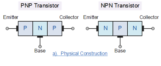
There are two types of bipolar transistor construction, PNP and NPN. This describes the physical arrangement of the P-type and N-type semiconductor materials they were made from.
The bipolar transistor basic construction consists of two P-N junctions producing three connecting terminals. Each terminal is given a name to distinguish it from the other two. These three terminals are known and labelled as the Emitter (E), the Base (B) and the Collector (C), respectively.
Bipolar transistors control the amount of current flowing through them, from the Emitter to Collector terminals in proportion to the amount of biasing voltage applied to their base terminal. It therefore acts like a current-controlled switch.
The principle of operation of the two transistor types, PNP and NPN, is the same, except the biasing and the polarity of the power supply for each type.
Bipolar transistor construction
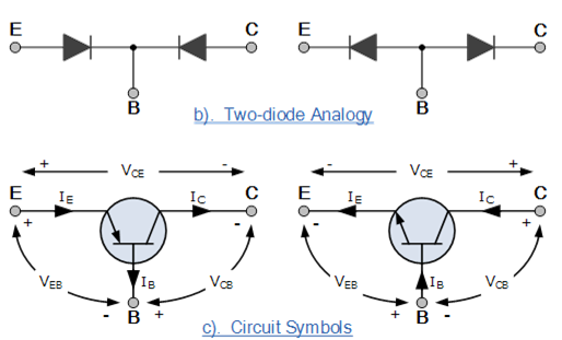
The images below show the physical construction, analogy and circuit symbols for a bipolar transistor. The arrow in the circuit symbol always shows the direction of “conventional current flow” between the base terminal and its emitter terminal.
The direction of the arrow always points from the positive P-type region to the negative N-type region for both transistor types, the same as for the standard diode symbol.
Bipolar transistor configurations
As the bipolar transistor is a three-terminal device, there are three possible ways to connect it within an electronic circuit. One terminal is common to both the input and output.
Each method of connection responds differently to its input signal within a circuit, as the static characteristics of the transistor vary with each circuit arrangement.
- Common Base Configuration: has Voltage Gain but no Current Gain.
- Common Emitter Configuration: has both Current and Voltage Gain.
- Common Collector Configuration: has Current Gain but no Voltage Gain.
The common base (CB) configuration
In the common base, or grounded base, configuration, the base connection is common to the input and output signals.
The input signal is applied between the transistors base and the emitter terminals, while the corresponding output signal is taken from between the base and the collector terminals. The base terminal is grounded or can be connected to some fixed reference voltage point.
Since the input current is the sum of both the base current and collector current, we would define the current gain for this type of circuit of “1” (unity) or less; in other words, the common base configuration “attenuates” the input signal.
The common emitter (CE) configuration.
In the common emitter, or grounded emitter, configuration, the input signal is applied between the base and the emitter. The output is taken from between the collector and the emitter.
This is the most common configuration used for transistor-based amplifiers and represents the “normal” method of bipolar transistor connection. The common emitter amplifier configuration produces the highest current and power gain of all the three bipolar transistor configurations.
This is mainly because the input impedance is LOW as it is connected to a forward biased PN-junction, while the output impedance is HIGH as it is taken from a reverse biased PN-junction.
The common collector (CC) configuration
In the common collector, or grounded collector, configuration, the collector is connected to ground through the supply. Therefore, the collector terminal is common to both the input and the output.
The input signal is connected directly to the base terminal, while the output signal is taken from across the emitter load resistor. This type of configuration is commonly known as a voltage-follower or emitter-follower circuit.
The common collector, or emitter follower configuration, is very useful for impedance matching applications because of its very high input impedance, in the region of hundreds of thousands of Ohms while having a relatively low output impedance.
Keep an eye out for our next articles where we dive into analogue and digital electronics.
Interested in our courses?
You can read more about our selection of accredited online electrical and electronic engineering courses here.
Check out individual courses pages below:
Diploma in Electrical and Electronic Engineering
Higher International Certificate in Electrical and Electronic Engineering
Diploma in Electrical Technology
Diploma in Renewable Energy (Electrical)
Higher International Diploma in Electrical and Electronic Engineering
Alternatively, you can view all our online engineering courses here.
Recent Posts
Civil Engineering Courses and Diplomas: Topics, Skills and Career Routes
Civil Engineering Courses and Diplomas: Topics, Skills and Career Routes Introduction Civil engineering is the backbone of modern society. From roads and bridges to skyscrapers and water systems, civil engineers design, build, and maintain the infrastructure that keeps the world running. If you’re considering a civil engineering course or diploma, understanding what it covers is […]
What Is a Diploma in Engineering? Courses, Levels and Career Routes Explained
What Is a Diploma in Engineering? Courses, Levels and Career Routes Explained Introduction Engineering shapes the world around us, from the buildings we live in to the technology we use every day. But for many aspiring engineers, the biggest question is not whether to pursue engineering, but how to start. Traditional university degrees are not […]
Engineering Courses: How to Choose the Right Route for Your Career
Engineering Courses: How to Choose the Right Route for Your Career Introduction Choosing an engineering course can feel like standing at the beginning of several different roads, each leading towards a different kind of future. One route may lead into mechanical systems and manufacturing. Another may lead towards aircraft, infrastructure, electronics, computing, renewable energy or […]